4 Bit Parallel In Serial Out Shift Register Timing Diagram. This register can be used to store and shift a 4 bit word with the write shift ws control input controlling the mode of operation of the shift register. Here control line is used to select the functionality of the shift.
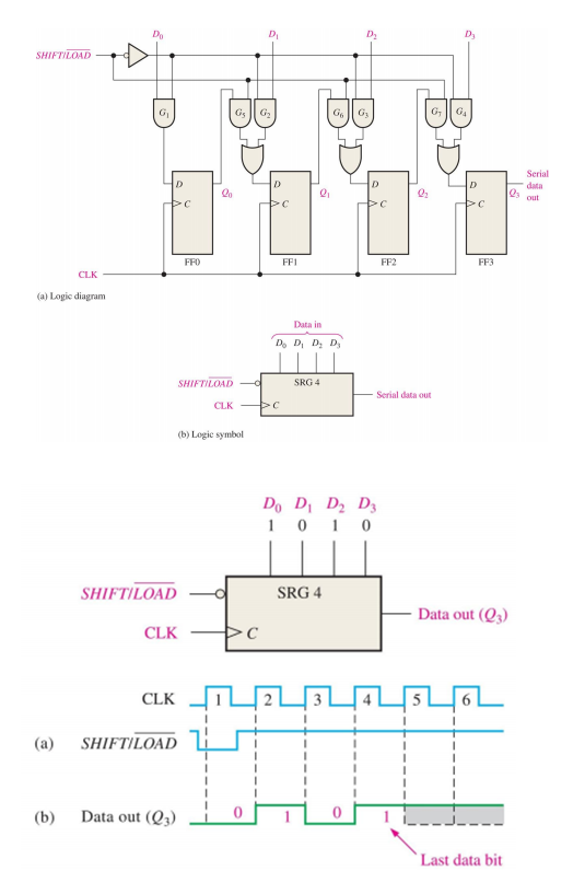
Serial in serial out shift registers delay data by one clock time for each stage. In parallel in serial out piso shift registers the data is loaded onto the register in parallel format while it is retrieved from it serially figure 1 shows a piso shift register which has a control line and combinational circuit and and or gates in addition to the basic register components fed with clock and clear pins. 4 bit parallel in serial out shift register b.
We have already looked at the internal details of the sn74ls395a see above previous figure 74ls395 parallel in parallel out shift register with tri state output.
The shift register which allows parallel input and produces serial output is known as parallel in serial out piso shift register. That covers the parallel out part. Be sure to include the clock signal in the timing diagram. 4 bit parallel in to serial out shift register as this type of shift register converts parallel data such as an 8 bit data word into serial format it can be used to multiplex many different input lines into a single serial data stream which can be sent directly to a computer or transmitted over a communications line.
