Clocked Rs Flip Flop Timing Diagram. By adding two extra nand gates the timing of the output changeover after a change of logic states at s and r can be controlled by applying a logic 1 pulse to the clock ck input. This is a non clocked device that consisting of two cross connected 2 input nand gates may also be made from other gates.
In this article we will discuss about sr flip flop. Clocked rs flip flop. This is known as a timing diagram for a jk flip flop.
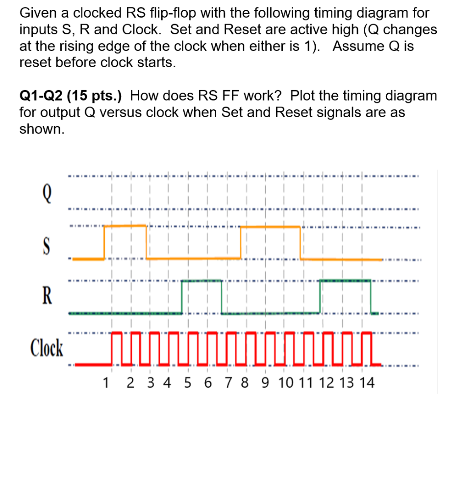
Clocked rs flip flop.
Construction of sr flip flop there are following two methods for constructing a sr flip flop by using nor latch. In the clocked r s flip flop the appropriate levels applied to their inputs are blocked till the receipt of a pulse from an other source. This is known as a timing diagram for a jk flip flop. It stands for set reset flip flop.
