Cmos Nand Gate Stick Diagram. Layouts unit ii circuit design processes the cmos nor gate. Two input nor gate.
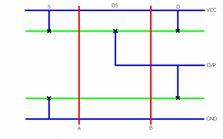
Figure below shows the schematic stick diagram and layout of two input nand gate implemented using complementary cmos logic. Draw the stick diagram for two input nand gate. Eulerpaths cmos vlsi design slide 3 complex circuit layouts single diffusion runs multiple diffusion runs c a b ab eulerpaths cmos vlsi design slide 4 4 input nand gate sticks layout i1 i2 i3 i4 out step 1.
The circuit diagram of the two input cmos nand gate is given in the figure below.
Draw the stick diagram for 2 1 mux using. Eulerpaths cmos vlsi design slide 3 complex circuit layouts single diffusion runs multiple diffusion runs c a b ab eulerpaths cmos vlsi design slide 4 4 input nand gate sticks layout i1 i2 i3 i4 out step 1. Two input nor gate. Figure below shows the schematic stick diagram and layout of two input nor gate implemented using complementary cmos logic.
