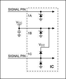
Esd Protection Circuit Design. Through suitable substrate triggering design on the device structure this proposed input esd protection circuit can successfully protect the thinner gate oxide 50 å of the input stage in a 0. Connected in parallel with the signal lines the suppressors clamp the esd voltage and shunt the majority of the esd current away from the data line and the protected chip to the appropriate reference.
Oops Practical Esd Protection Vs Foolhardy Placebos from www.maximintegrated.com
Electrostatic discharge esd protection design is needed for integrated circuits in cmos technology. Loops in a line can give rise to unwanted current arising from induction. In this esd protection circuit the nmos s gate is grounded to keep it off during normal circuit operation.
In this esd protection circuit the nmos s gate is grounded to keep it off during normal circuit operation.
Electrostatic discharge esd protection design is needed for integrated circuits in cmos technology. Dynamic resistance r dyn. However these esd protection devices come with some unwanted side effects. Care should be taken to ensure that no loops exist.