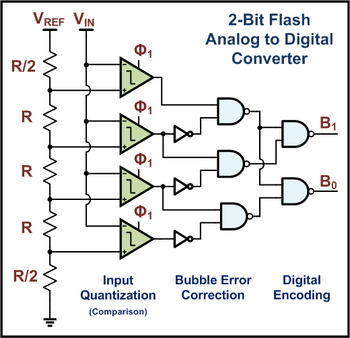
Flash Type Adc Circuit Diagram. The priority encoder generates a binary number based on the highest order active input ignoring all other active inputs. A typical conversion time of three bit flash analog to digital converter is 33 ns.
Thermometer code to binary encoder vn v3 v2 v1 vin d2 d3 dk d1 gain booster circuit gain booster gain booster gain booster gain booster figure 1 block diagram of the proposed tiq based flash adc. The entire digital output word is present just after the propagation delay time of comparators and the encoding logic gates. Hence flash type adc is the fastest adc.
The circuit is found to be working satisfactorily.
The circuit diagram of a 3 bit flash type adc is shown in the following figure the 3 bit flash type adc consists of a voltage divider network 7 comparators and a priority encoder. A typical conversion time of three bit flash analog to digital converter is 33 ns. The circuit diagram of a 3 bit flash type adc is shown in the following figure the 3 bit flash type adc consists of a voltage divider network 7 comparators and a priority encoder. Thermometer code to binary encoder vn v3 v2 v1 vin d2 d3 dk d1 gain booster circuit gain booster gain booster gain booster gain booster figure 1 block diagram of the proposed tiq based flash adc.
