Jk Flip Flop Timing Diagram. Jk flip flop circuit diagram and explanation. Actually a j k flip flop is a modified version of an s r flip flop with no invalid output state.
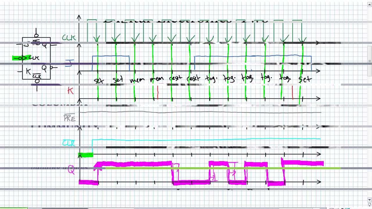
In our previous article we discussed about the s r flip flop. 3 bit ripple counter using jk flip flop truth table timing diagram. The circuit diagram of the jk flip flop is shown in the figure below.
Also we have used led at output the source has been limited to 5v to control the supply voltage and dc output voltage.
3 bit ripple counter using jk flip flop truth table timing diagram. No bubble would indicate a positive edge triggered. Hence we can assume that the master slave j k flip flop is a synchronous electric device because it only sends data at specific clock input timing. The small triangle on the clock input indicates that the device is edge triggered.
