Jk Flip Flop Timing Diagram Calculator. While this implementation of the j k flip flop with four nand gates works in principle there are problems that arise with the timing. The inputs labelled j and k are shown on the left.
J K Flip Flop from hyperphysics.phy-astr.gsu.edu
This circuit is a jk flip flop. The s and r inputs of the rs bistable have been replaced by the two inputs called the j and k input respectively. The first step in converting a jk to sr flip flop would be to write a jk to sr conversion table as shown in figure 1.
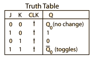
Jk flip flop timing diagram from the truth table above one can arrive at the equation for the output of the j k flip flop as table ii.
When j k 1 the output is toggled from high to low or low to. When j k 1 the output is toggled from high to low or low to. This circuit is a jk flip flop. It only changes when the clock transitions from high to low.