Jk Flip Flop Timing Diagram Explanation. Jk flip flop construction logic circuit diagram logic symbol truth table characteristic equation excitation table are discussed. Also we have used led at output the source has been limited to 5v to control the supply voltage and dc output voltage.
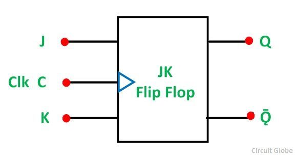
J corresponds to a set signal and k corresponds to a reset signal. Jk flip flop timing diagram from the truth table above one can arrive at the equation for the output of the j k flip flop as table ii. Jk flip flop construction logic circuit diagram logic symbol truth table characteristic equation excitation table are discussed.
When both the inputs s and r are equal to logic 1 the invalid condition takes place.
The old two input and gates of the s r flip flop have been replaced with 3 input and gates and the third input of each gate receives feedback from the q and q outputs. Timing diagram for the positive edge triggered d flip flop. J corresponds to a set signal and k corresponds to a reset signal. The four inputs are logic 1 logic 0.
