Pipo Shift Register Timing Diagram. Directly above is the ansi symbol for the 74ls395. The block diagram of 3 bit pipo shift register is shown in the following figure.
Here control line is used to select the functionality of the shift register amongst shift or load at a given instant of time. The block diagram of 3 bit pipo shift register is shown in the following figure. We will compare siso sipo piso and pipo shift registers of 4 bit in size.
Shift register sipo pipo mode contribute.
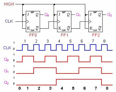
This sequential device loads the data present on its inputs and then moves or shifts it to its output once every clock cycle hence the name shift register. The block diagram of 3 bit pipo shift register is shown in the following figure. Here each flip flop stores an individual bit of the data in appearing as its input ff 1 stores b 1 appearing at d 1. Parallel in parallel out pipo shift registers are the type of storage devices in which both data loading as well as data retrieval processes occur in parallel mode.
