Sr Flip Flop Timing Diagram. In this video i have solved an example on sr latch timing diagram. Notice that the output of each gate is connected to one of the inputs of the other gate giving a form of positive feedback or cross coupling.
Edge triggered flip flop contrast to pulse triggered sr flip flop pulse triggered. Now draw the s r latch with nor gates write initial values near corresponding letters s 0 r 0 q 0 qn 1 change s to 1 and try to understand what changes you see. Timing diagram of sr flip flop helps to understand the.
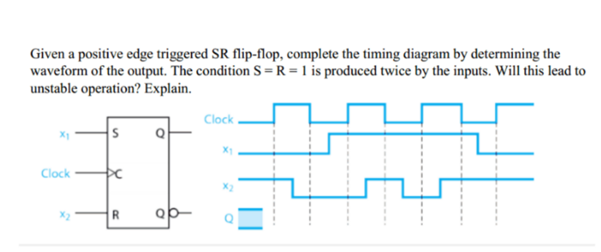
Read input while clock is 1 change output when the clock goes to 0.
If you struggle look at the timing diagram you shared. 11 sr flip flop timing diagram. If you struggle look at the timing diagram you shared. In the first timing diagram when s becomes 1 after 10ns qn becomes 0 and 10ns later q becomes 1.
