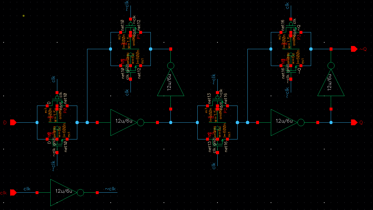
D Flip Flop Schematic In Cadence. Basically i am designing d flip flop. D flip flop can be built using nand gate or with nor gate.
Quartus ii allows a number of methods of design entry. D flip flop design practice mycad 4 inverter schematic and symbol 1 0 0 1 in out input output logic symbol schematic truth table l 0 2um w 1 6um l 0 2um. Using cadence environment tsmc 180nm tech.
Basically i am designing d flip flop.
Octal d type edge triggered flip flop with 3 state outputs. While doing my pre layout simulations not getting the output q for the inputs. Octal d flip flop with clock enable. Due to its versatility they are available as ic packages.
